Basic information about memory chips and programming
We receive frequent inquiries on memory chips and are repeatedly forced to note that there is still a very high requirement for information in this area. For this reason, we are now making the basic information for programming memory chips, such as eproms/eeproms and Flash chips, public here. In particular, we will discuss the various types of memory chips and compare what the 27C, 28C or 29F series, for instance, can and cannot do.
- What is a memory chip?
- Organization of a memory chip
- EPROM memory chips (27 / 27C...)
- EEPROM memory chips (28C...)
- FLASH EPROMS (28F..., 29C..., 29F...)
- Serial EEPROMS (24C..., 25C..., 93C...)
- RAM (52..., 62...)
- NVRAM (48Z..., DS12..., XS22...)
- Microcontroller
- Erasure of eproms with ultraviolet light
- Memory chip names and how to find replacement chips
What is a memory chip?
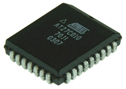
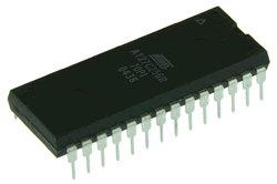
A memory chip is an electronic component which can store a program, data or both. In this context, a program is a series of commands (command string) for a microprocessor (= computing unit). Data could consist, for instance, of temperature values taken by a temperature measurement system, or any other data.
The program / data is stored in the memory chip by a series of numbers - zeros and ones (=bits). A Bit can either be a zero (0) or a one (1). It is difficult for a person to gain an overview over these Bits; therefore, they are gathered into groups. Sixteen bits are a "Word", eight bits are a "Byte" and four bits are a "Nibble".
The most commonly used term is the Byte, which contains 8 bits and can accept 2 to the 8th power = 256 different values. In order to represent these, the hexadecimal number system is used. This is based on a number of 16 and uses the digits 0 to 9 and additionally, A to F. Therefore, two digits can also accept 256 values (from 00h to FFh, wherein the small "h" only identifies the hexadecimal number). We would like to direct those who need more precise information about the number systems to suitable other locations.
The terms Kilo and Mega with regard to Bytes were also adapted to the binary nature (zero or one) of the digital systems. Here, Kilo means 1024 (= 2 to the 10th power) and Mega means 1024 * 1024 = 1048576. Therefore a Kilobyte is 1024 Bytes and a Megabyte is 1048576 Bytes.
Organization of a memory chip
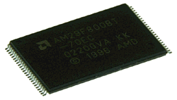
For the 8 Bit memory chips (the most common type) the Bits are put together in a Byte (= 8 bits) and stored under an "address". The Bytes can be accessed at this address and then the eight bits of the accessed address are output on its eight data ports. For example, in an 8-megabit chip like the 27c801, there are altogether 1048576 bytes (= 8388608 bits). Each Byte has its own address, numbered from 00000h through FFFFFh (corresponding to the decimal 0 to 1048575).
Aside from the 8 Bit memory chips, there are also 16 Bit memory chips, serial 1-Bit memory chips and (rarely/old) 4 Bit chips.
EPROM memory chips (27 / 27C...)
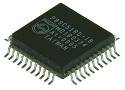
EPROM stands for Erasable Programmable Read Only Memory. What does this mean in detail?
"Erasable" means that the data on it can be removed. With these chips, erasure is carried out by exposure to intensive ultraviolet light in the area of 254 nm wavelength. We deal with erasing eproms with UV-C light in further detail below.
"Programmable" means that a program or data can be programmed (burned) into this chip. For programming, a programming device such as the Batronix Eprommer or the Galep-4 is required.
"Read Only Memory" means that this type of memory can be read out but not programmed in the target device.
This memory type can be burned (programmed) by a programming device and then retains its data until an erasing device erases it. During the programming process, any desired number of bits from one to zero can be programmed. Eproms can also be programmed repeatedly without being erased as long as the bits are only changed from one to zero or remain on zero. To change a bit from zero to one, erasure is necessary.
Since the quartz glass window required for erasing the chip with UV-C light is a big part of the production costs for the chip, this chip is available with and without this window. Without the window, the chip cannot be erased using UV-C light. The eproms with windows are also called UV eproms; the ones without are called OTP (=One Time Programmable) eproms.
After programming an erasable eprom with UV-C light, the glass window should be closed with a sticker so no sunlight can enter. Sunlight also contains components of UV-C light and can eventually erase data from the eprom.
In the name of an EPROM, the "C" after the 27 indicates that it is a CMOS EPROM (CMOS=Complimentary Metal Oxide Semiconductor). These require a much lower performance than the old NMOS EPROMS and can function with lower programming voltages (12.5 volts) (NMOS=N-channel Metal Oxide Semiconductor). Since both chips are otherwise compatible, the old NMOS EPROMS can be replaced with CMOS EPROMS of the same size (e.g. a 2764 can be replaced by a 27C64).
EEPROM memory chips (28C...)
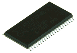
The name EEPROM stands for Electrically Erasable Programmable Read Only Memory. These are constructed like EPROMS, but allow the erasing of individual bytes or the entire memory space electrically without UV light. Since individual bytes can be erased without erasing everything, these individual bytes can be overwritten, in effect. However, with an EEPROM, the burning process clearly takes longer than with an EPROM - up to several milliseconds per byte. To make up this disadvantage, EEPROMS like AT28C256's were equipped with a function for the programming of so-called blocks. In this process, 64, 128 or 256 bytes at once are loaded into the memory chip and programmed simultaneously as a block. This clearly shortens programming times.
The additional internal cost for electrical erasure as well as the block writing function, if desired, makes the EEPROMS more expensive than the EPROMS.
FLASH EPROMS (28F..., 29C..., 29F...)
These chips can be erased electrically - completely or by the block - and some - like the AT28C... with the EEPROMS) can be programmed by the block as well. The Flash EPROMS, however, cannot always be used as a replacement for a normal eprom. Reasons include, for instance, that the Flash eproms, even the ones with a small amount of memory space, are only available in housings with 32 or more pins. A 28F256 with 32 pins is therefore not pin compatible to a 27C256 with 28 pins and the same memory capacity.
Serial EEPROMS (24C..., 25C..., 93C...)
With these chips, serial means that data output and address naming takes place bit by bit (=serially). This means that only one bit at a time can be accessed, and the accessed address must be communicated bit by bit as well, but it has the major advantage that the serial EEPROM comes with a small 8-pin housing. These chips are therefore popular when space or accessing cables are to be saved and no large amounts of data or high speeds are required.
RAM (52..., 62...)
The name RAM stands for "Random Access Memory" (= memory with selectable access). These memory devices can be written to very quickly (in this case, it is generally referred to as writing, not burning) and each byte can be overwritten just as quickly and easily, i.e. it does not need to be erased first. The disadvantage of this technology is that the chips lose their memory space when the power supply is cut off.
NVRAM (48Z..., DS12..., XS22...)
The name NVRAM stands for Non Volatile Random Access Memory. These chips have the major advantages of the RAM chips (very high speed and easy overwriting of existing data) and retain their data when power is cut off.
This can be achieved in two ways: The first group removes the disadvantage of the original RAMS with a built-in battery that protects the memory space from losing its data when the power is cut off. According to the manufacturer, the battery lasts for ten years according to type.
The second group has an equally large EEPROM and when the power is cut off, it stores all data from the RAM on the EEPROM. When the power is restored, data are EEPROM copied back into the RAM. The advantages of fast RAM access and easy overwriting remain.
Microcontroller
A microcontroller is a complete system, consisting of the CPU (computing unit/microprocessor), the programming memory (FLASH or EPROM), working memory (RAM) and in/output on a chip. These chips are put into many devices as "mini-PC's" and guide, for instance, printers, heaters, microwaves, alarm clocks etc..
Erasure of eproms with ultraviolet light
With these chips, erasure takes place by exposure to intensive ultraviolet light in the area of 254 nm wavelength. Since UV-C light is very dangerous to the eyes and also carcinogenous, these chips are erased in special eprom erasure devices. These only allow the light to be turned on after the housing is closed. When the housing is opened, the light is immediately switched off. Erasure takes 5 to 25 minutes, varying with light intensity and other conditions.
We have often been asked whether eproms can also be erased with a face-tanning device or similar. This is, however, not possible, since the UV-C wavelength of the light is filtered out in these devices. Erasure using daylight is, on the other hand, possible, since sunlight contains the required wavelength. This is, however, not of practical use since it would require a few weeks of bright sunshine.
Memory chip names and how to find replacement chips
The name of a memory chip contains the abbreviation for the manufacturer, the technology, the memory size, the fastest permitted accessing speed, the temperature range, the form of housing as well as further internal manufacturer's data. Different manufacturers often use very different names, however the chips with similar data under the various manufacturers are usually compatible.
It takes practice to correctly interpret the name of a memory chip. But it generally does not take long to learn and once learned, it is normally easy to determine a replacement type. A replacement type should utilize the same technology (EPROM/ EEPROM/ FLASH/ etc.), have the same size of memory and the same or a shorter access time and if applicable, the same or a better temperature range.
In the case of an existing memory chip, one first looks for the technology description on the housing, e.g. 27C, 28C, 29F etc.. An abbreviation for the manufacturer is usually in front of it (e.g. AT for Atmel). After it, one finds the memory size in bits, which can be given in different ways according to the manufacturer:
Selected possible memory sizes:
- 16 = 16 KBit
- 32 = 32 KBit
- 64 = 64 KBit
- 128 = 128 KBit
- 256 = 256 KBit
- 512 = 512 KBit
- 1001 or 010 = 1 MBit
- 2001 or 020 = 2 MBit
- 4001 or 040 = 4 MBit
- 8001, 080 or 801= 8 MBit
- 016 = 16 MBit
It should be noted that memory size is given in bits and not in bytes. After the memory size, there may be a version name, such as "B", and then a hyphen. After the hyphen, the fastest permitted access speed is given in nanoseconds (1/1000000000 second). This is the maximum delay time between the inputting of an address and the outputting of the data to the ports of the memory chips. This entry takes some getting used to as well, since it is given in two digits:
Selected possible access speeds:
- 45 = 45 ns
- 60 = 60 ns
- 70 = 70 ns
- 90 = 90 ns
- 10 = 100 ns
- 12 = 120 ns
- 15 = 150 ns
- 20 = 200 ns
- 25 = 250 ns
After the maximum access speed, there is an abbreviation for the housing type and the permitted temperature range. Since these can vary, one should check the data sheet if in doubt. Data sheets can be easily located via search engines such as www.google.com, using the term for the chip + the word "datasheet" as search terms (for example, 27c256 +datasheet).
Knowing this, the label M27C1001-10F1 now tells us that it is an eprom (=27C) with 1 MBit of memory (=1001) with an access time of 100 ns (=10) in the DIP housing (=F) with a permissible temperature range of 0 to 70 degrees Celsius (=1).
In a further line of labeling on the memory chip, one then finds the date of manufacture (the date code). This is the year (given in two digits) and the calendar week. A chip with a date code 0109 is therefore from the 9th calendar week in 2001.
